

Microwave Furnaces for Silicon Recycling and Production
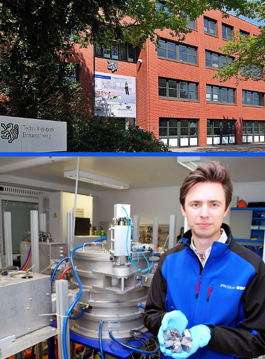
JPM Silicon is headquartered at the Technology Park Braunschweig in Germany, which provides office infrastructure and the space needed for equipment and experiments. The company has grown to 10 young highly qualified employees.
It all began in 2005 when Jan-Philipp Mai - a high school student at that time - conducted experiments with a store bought microwave oven and a few other components to melt silicon. Since silicon has a melting point of 1,414°C, the challenge was daunting. But he succeeded and founded JPM Silicon in 2010 to commercialize the idea.
As CEO, Jan-Philipp (left) has raised a substantial amount of seed money from family, friends, institutions and early investors. After a few iterations, technology solutions based on the initial idea emerged with the potential to fill commercial voids:
Production of Solar Silicon
Production of solar silicon at much lower cost as currently possible.
Recycling of Silicon of Powder and Fines
Turning silicon powder and fines into pellets and chunks with purity levels of metallurgical silicon.
Raw Material Testing
Characterization of quartz and coal for the production of raw/metallurgical silicon faster and at much lower cost with reliable analytical details.
Consulting - Analytical Software Package "Industry 4.0"
Modeling the material flow of a factory to minimize waste streams based on a scientific approach.
HOW SILICON POWDER CAN BE RECYCLED WITH A MICROWAVE MELTING FURNACE
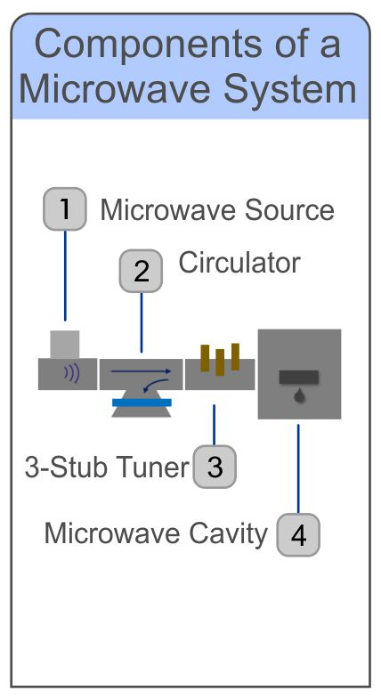
Why can silicon be melted with a microwave? Microwave energy is absorbed by the silicon particles and the heating starts from the inside out. Allmost all the microwave energy is transformed directly into heat. This concept allows high heating rates of
250 K/min and precise control.
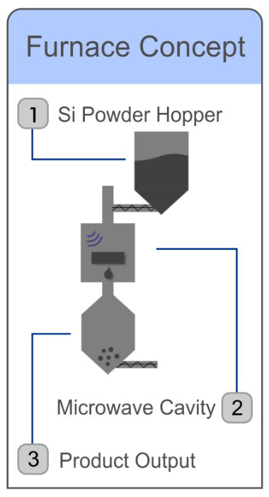
Silicon powder/fines are loaded into the hopper. From there they are transported continuously into the microwave cavity. Following gravity, the melted silicon passes a filter and is then directed to solidify in the output unit. The size of the solidified pieces can be adjusted from pellets to chunks.
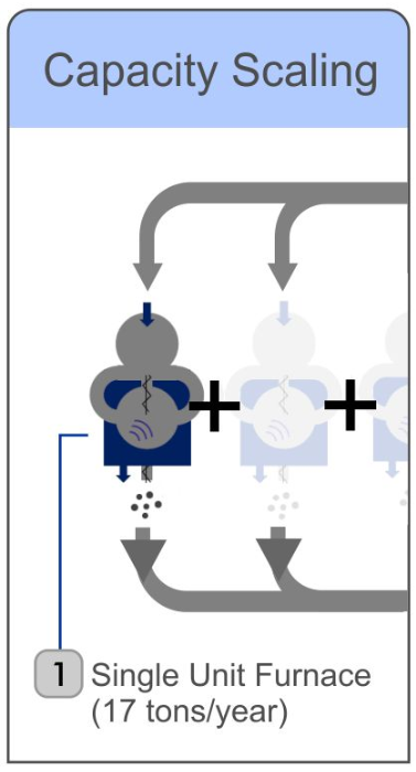
The smalest furnace produces 17 tons of silicon per year in a 24/7 fashion. Consumables are filters and an inert gas at the rate of 3 liters/min. The unit is compact and easy to maintain. The output capacity can be scaled by adding furnaces and connecting them to a common input/output system.
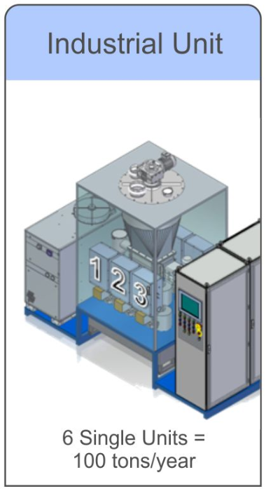
The industrial unit represents the base configuration for mass production. The output is scaled by adding industrial units. The unit is fully automated. One operator and one technician are required for 8 units in a three shift working environment. The OPEX lies at about 550 €/ton.
Production of Solar Silicon
Silicon for the solar industry has to be as pure as 6N or better, which can be achieved in two steps: (i) the production of metallurgical silicon with an arc furnace and (ii) refining the metallurgical silicon through its transformation into volatile liquids (silane, trichlorosilane or tetrachlorosilane), then destillation to purify it and deposition as a solid in a CVD process (Siemens reactor). That does not only sound expensive, it is. A few companies came up with alternative methods that actually manage to reach 6N without involving the above mentioned steps.
JPM has developed IP for a technology to produce solar grade silicon with their microwave technology. The key is to find the right combination of starting materials and a process with a purification step leading to > 6N.
The advantage as compared to other methods is that melting material with the microwave furnace is much more efficient, the process tightly controlled and hence less expensive. The technology can be scaled for high volume production and needs less space. It can be run in a continuous fashion to produce silicon chunks directly and continously. No breaking or crushing would be necessary.

Silicon Recycling
Silicon powder is a byproduct in a number of processes in silicon and wafer factories: (i) production of metallurgical or raw silicon (ii) polysilicon production in a fluidized bed reactor, (iii) crushing polysilicon rods to produce silicon chunks, (iv) grinding and sawing silicon.
Loose silicon powder cannot be melted in a crucible for cyrstal growth. Over time, several heating methods - resistive, inductive or electron beam heating - had been tried but turned out to be economically not feasable.
With JPM's microwave furnace silicon powder can be melted efficiently. The furnace works in batch or continuous mode producing silicon pieces of adjustable size, from small pellets to chunks and even small ingots. The furnace can be equipped with a purification unit that improves the silicon quality.
General Features
- Input: Silicon powder in the µm to mm range
- Output: Silicon pellets, granules, or small ingots
- Compact furnaces scalable to continuous (inline) production capacities of thousends of tons
- Discontinuous operation possible due to short start-up time and therefore suitable for smaller factories
- Easy installation and fully automated
- Energy efficient with optional refining unit
- OPEX to produce one ton of silicon from powder is 1/5 to 1/3 of the market price for a ton of metallurgical silicon
Raw Material Testing
Silicon is manufactured by reducing mined quartz to silicon in an arc furnace, which has a diameter of 5 to 10 meters and works at temperatures in access of 2,000°C. Commenly used reducing agents are coal, charcoal and wood chips, which hints that the process is not an exact science. The yield of the chemical reaction and the quality of the produced silicon depend on the chemical composition and structural properties of the materials. Hence, tests have to be run to determine the optimal quartz/coal composition. This is carried out in an arc furnace. Tons of materials are needed for that and it takes hours for the silicon to come out. Then it has to be analyzed.
JPM has developed a method involving their microwave melting technology to predict the quality of the silicon end product before it is produced in the arc furnace. This is achieved by letting react small samples of the availabe quartz and coal independently from each other, with their respective well characterized and pure reaction agent (quartz with carbon, coal with SiO2).
The solidified samples are then analyzed by means of ICP mass spectroscopy. The results allow to predict the expected silicon yield and quality in the lab within a few hours. A list of all the impurities present in the produced materials is generated.
JPM carries out the tests as a service and provides a detailed report. Several well known silicon producers are using JPM's characterization service.
Consulting - Industry 4.0 for Your Factory
With their proprietary software package designed to optimize the material streams in silicon factories, JPM is bringing Industry 4.0 or what is also called the "fourth industrial revolution" to you. Behind this term hides a concept that everybody implicitely knows about but which in its ultimate consequence is installed in only few companies.
Most factories run automated equipment, collect some sytem data and performance values but do not monitor the physical material streams. But that is where you can loose money, i.e. when material in the workflow from input to output gets lost and you don't know that it happens, where it happens, why it happens and in what quantities it happens. If you do not know all that, what makes you so sure that your bottom line is where it should be?
This is where JPM comes in. JPM starts by identifiying all economically relevant material flows in the production line and assigns a monetary value to each. The entire material flow will be modeled with JPM's proprietary software to identify and define interdependencies. From the balance of the material flow derived from this analysis, JPM develops strategies for optimization that they implement together with you.
To make these efforts last, customers can acquire JPM's software solution tailored to your production line. With it the material flow for all processes can be monitored continously and quantitatively in real time. The software sends out an alert when problems emerge and a team can be deployed to troubleshoot and rectify them immediately.
Where is JPM Silicon located? JPM is headquartered in Braunschweig, Germany. The next international airport is Hannover (HAJ). From there it is a 1 hour ride by car. The town is well known for its university and research institutes. The Physikalisch-Technische Bundesanstalt (equivalent to NIST in the US) is located here.